Module 011: Writing Sequential Logic
Module 011: Writing Sequential Logic
The previous module already covered how we can implement complex combinational logic. Now, move from combinational logic (no memory, outputs depend only on inputs) into sequential logic (where outputs depend on both current inputs and stored past values). This is where we introduce flip-flops, registers, and the all-important clock. We will use a similar-looking construct from the previous module: the always @(posedge clk) block.
The always @(posedge clk) Block
Digital systems often need to remember information and update it in steps, synchronized to a clock signal (clk). In Verilog, this is described with the always @(posedge clk) block, which means: “Run this block whenever the clock has a rising edge.” Whenever we have a logic element that gets evaluated only during the edge of a signal, we are modelling a flip-flop, the basic storage element in sequential circuits.
posedge is a keyword indicating the sensitivity to the rising edge of the signal named after the keyword (in this case, clk). negedge is also another keyword that can be used to signify sensitivity to the falling edge of the same signal.
Example: Simple Register
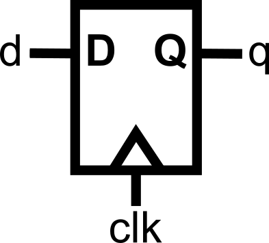
qis declared asreg(because it is being assigned inside an always block).- We use
<=instead of=for the signal assignment.
<= vs. = Assignments
Inside a sequential (always @(posedge clk)) block, we use a different assignment (<=).
- Use
<=in sequential (always @(posedge clk)) blocks. - Use
=in combinational (always @(*)) blocks.
You could technically use the assignments interchangeably; however, there are intricate details regarding how assignments are evaluated that differentiate the two forms. For this crash course, to keep things simple and to maintain the concurrent timing model, just follow the guidelines above as the golden rule. No exemptions.
This keeps your design consistent and avoids timing bugs.
More Complex Sequential Logic
We already know if-else from combinational logic, as presented in the previous module. Now let’s see it inside a clocked block.
Here’s an up-down counter:
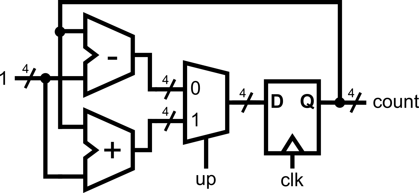
For every positive edge of the clock, the module updates the count output by +1 or -1, depending on the input signal up. Since the update happens on every positive edge of the clock, flip-flops are inferred by the module description.
Since we are now in the sequential logic domain, assignments such as count <= count + 1; where the same signal appears in both the left (output) and right (input) side, are possible. Loops within sequential logic are possible because the path propagation is being controlled by the clock trigger.
On the contrary, count = count + 1; should not be done in the combinational logic domain (when using always@(*)), as this would infer a combinational loop, which is not realizable in hardware.
.png)
Inferred Latches in Sequential Logic
In combinational logic (always @(*)), forgetting to assign a signal in all cases leads to an inferred latch, as described in Module 0x2. This is usually unintentional and dangerous because latches can create feedback loops and unpredictable timing. Combinational feedback loops should not exist in a properly designed digital system.
But in sequential logic (always @(posedge clk)), holding the old value is expected behavior. In fact, it’s how registers naturally work! Typical registers have write enable ports that allow them to either capture new data or hold the previous value every clock trigger. This can be properly modeled in Verilog.
Example A: Implicit Register Hold (Inferred Latch)
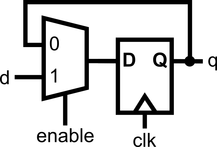
Even though q is not assigned in the else, this is fine in sequential logic:
- If
enableis 0, the registerqsimply doesn’t update — it keeps its old value.
Example B: Explicit Register Hold
This synthesizes to the same hardware as Example A. In sequential logic, both versions are correct and safe, because registers naturally remember their value across clock cycles.
- In combinational logic, missing assignments → unintended latches (bad).
- In sequential logic, missing assignments → “hold register value” (fine).
Resetting Values
Registers/flip-flops don’t have defined values at power-up. If you don’t set them, simulators may show them as “X” (unknown). This can be problematic since we are now allowing looped assignments, such as count <= count + 1; from earlier. If the value of count is not initially defined, the assignment will also not be defined, no matter how many clock triggers pass. Therefore, there is a need to properly reset the sequential logic.
We usually add a reset input that forces signals to known values. This can be done synchronously (with the clock) or asynchronously (immediately).
Example: Synchronous Reset
Example: Asynchronous Reset

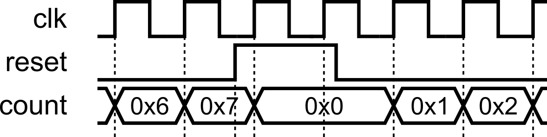
Always put reset at the top of the if-else hierarchy, so it takes the highest priority. In sequential always @(posedge clk) blocks, put the reset check at the top (and alone, that is, no other logic should be present aside from reset) of the if-else hierarchy: write if (reset) to initialize state, and place all other behavior under the else (nest further if/else as needed). This makes reset dominant and prevents any peer logic at the top level.
Here’s the up/down counter from the previous section with the additional asynchronous reset to illustrate the described reset hierarchy.
module updown_counter(
    input clk,    input nrst,                         // low-asserted reset
    input up,                           // 1 = count up, 0 = count down
    output reg [3:0] count              // 4-bit output to hold the current count
);
    always @(posedge clk or negedge nrst) begin
        if (!nrst) begin               // negedge reset -> low-asserted reset
            count <= 4'b0000;
        end else begin                  // the rest of the logic is under 'else'
            if (up)
               count <= count + 1;
            else
               count <= count - 1;
        end
    end
endmodule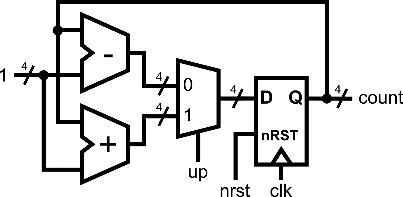
Concurrency Reminder
When we write an always @(posedge clk) block, every assignment inside that block describes a register. Each of those registers updates its value once per clock edge. Since the positive edge of the clock is a single time instant, therefore, all the registers will update at the same time.
Consider the following example:
.png)
At first glance, this might look like programming, where instructions run one after another. You might expect a to become b, and then b to immediately become that new value of a. But that’s not how hardware works.
Here’s what really happens:
- At the rising edge of
clk, all right-hand sides (banda) are read at the same time. These are the old values ofaandbfrom before the clock edge. - Each register (
aandb) schedules its update to the new value. - After the clock edge, all updates are applied concurrently.
So if a = 4'b1010 and b = 4'b0101 just before the clock edge:
- The new
abecomes0101(oldb). - The new
bbecomes1010(olda). And yes, this means they swap values, but only because the old values were both checked before either was updated.
Because of concurrency in the evaluation of assignments
is equivalent to:
The order of the statements inside the block does not change the hardware. Each line creates a register, and all registers are updated together on the clock edge.
Key Points
- Every assignment in an
always@(posedge clk)block infers a register. Each<=line creates a storage element that holds its value until the next clock edge. - All registers check inputs at the same time. That’s why it’s the old values that get used for every assignment.
- All updates happen together. No one register updates “before” another; they all change in lockstep with the clock.
Putting It All Together
Here’s a complete example demonstrating pipelined multiplication, combining everything you have learned so far. Note how this example combines both combinational logic, assigned using always@(*), and sequential logic, assigned using always@(posedge clk).
module pipelined_mult4 (
    input  clk,
    input  rst,         // synchronous, active-high
    input  [3:0] a,     // multiplicand
    input  [3:0] b,     // multiplier
    output reg [7:0] p  // product (registered)
);

    // ---------------------------
    // Pipeline registers (current state). These will be assigned inside always@(posedge clk)
    // ---------------------------
    reg [7:0] a0, a1, a2, a3;    // shifted/extended multiplicand (8-bit)
    reg [3:0] b0, b1, b2, b3;    // shifting multiplier bits
    reg [7:0] s0, s1, s2, s3;    // running partial sums

    // ---------------------------
    // Next-state signals (combinational). These will be assigned inside always@(*).
    // ---------------------------
    reg [7:0] a1_n, a2_n, a3_n;
    reg [3:0] b1_n, b2_n, b3_n;
    reg [7:0] s1_n, s2_n, s3_n, s4_n;  // s4_n is the final sum for this cycle
    reg [7:0] p_n;
    reg [7:0] pp0, pp1, pp2, pp3; // partial products

    // -----------------------------------------------------------------
    // COMBINATIONAL: compute next-stage values from current registers
    // - Use '=' for assignments in combinational logic
    // - Each stage: form partial product (pp#) and update running sum (s#_n)
    // -----------------------------------------------------------------
    always @(*) begin
        // Stage 0 -> Stage 1
        pp0  = b0[0] ? a0 : 8'h00;
        s1_n = s0 + pp0;
        a1_n = a0 << 1;
        b1_n = b0 >> 1;

        // Stage 1 -> Stage 2
        pp1  = b1[0] ? a1 : 8'h00;
        s2_n = s1 + pp1;
        a2_n = a1 << 1;
        b2_n = b1 >> 1;

        // Stage 2 -> Stage 3
        pp2  = b2[0] ? a2 : 8'h00;
        s3_n = s2 + pp2;
        a3_n = a2 << 1;
        b3_n = b2 >> 1;

        // Stage 3 -> Final (s4)
        pp3  = b3[0] ? a3 : 8'h00;
        s4_n = s3 + pp3;

        // Registered product next value
        p_n  = s4_n;
    end

    // -----------------------------------------------------------------
    // SEQUENTIAL: register transfer on the rising edge
    // - Use '<=' for assignments in sequential logic. Every assignment creates a flipflop.
    // - New inputs are loaded into stage 0 while older data advances
    // -----------------------------------------------------------------
    always @(posedge clk) begin
        if (rst) begin           // synchronous reset for all flipflops
            a0 <= 8'h00; a1 <= 8'h00; a2 <= 8'h00; a3 <= 8'h00;
            b0 <= 4'h0;  b1 <= 4'h0;  b2 <= 4'h0;  b3 <= 4'h0;
            s0 <= 8'h00; s1 <= 8'h00; s2 <= 8'h00; s3 <= 8'h00;
            p  <= 8'h00;
        end else begin
            // Load fresh inputs into stage 0 each cycle
            a0 <= {4'b0000, a};  // zero-extend to 8 bits
            b0 <= b;
            s0 <= 8'h00;         // running sum starts at 0 for new inputs

            // Advance the pipeline (all happen together at this edge)
            a1 <= a1_n; b1 <= b1_n; s1 <= s1_n;
            a2 <= a2_n; b2 <= b2_n; s2 <= s2_n;
            a3 <= a3_n; b3 <= b3_n; s3 <= s3_n;

            // Final product register
            p  <= p_n;           // equals s4_n from this cycle’s combinational work
        end
    end

endmodule.png)
Combinational blocks (always @(*)) are always assigned with =.
Sequential blocks (always @(posedge clk)) are always assigned with <=. Every assignment will create a flipflop.
Note that all assignments are happening concurrently. We are describing hardware in Verilog, and we are merely describing the interconnections between wires and the logic happening between those wires.
In this module, we learned:
always @(posedge clk)for sequential logic.- Use
<=inside sequential blocks (Golden Rule). - Registers need reset values.
- If-else chains work for sequential decisions.
- All registers update together on the clock edge (concurrency still holds!).
Module Activity : The LFSR
This module’s activity is in this Jupyter Notebook. Line by line, you can execute the code in order to see how the environment works. I recommend pressing the Run all button at the top and giving it about 2 minutes to download all of the requirements. In the middle of the notebook, you’ll find a section where you need to fill in some verilog code. Time to show your stuff.
In programming, we usually take randomness for granted. It is simple to use programming libraries and packages to generate random numbers. However, under the hood, generating random numbers is really really difficult. Linear Feedback Shift Registers (LFSRs) allow hardware engineers to efficiently generate “random numbers”.
In this activity, your task is to implement a 4-bit Galois-type LFSR using the knowledge you’ve gained about writing sequential logic.